|
|
计算器程序
| 程序名称: |
Ftune3 |
| 平台: |
fx-9860GII fx-9750GII 其他 |
| 系统/软件要求: |
|
| 版本号: |
2.40 |
| 类型: |
其他 |
| 作者: |
Sentaro21 |
| 大小(K): |
56.3 |
| 更新日期: |
2020-02-21 |
| 描述: |
- |
| 已知缺陷: |
- |
| 源代码: |
开源/部分开源 » 其它许可协议(请注明) |
本帖最后由 ilm 于 2025-11-14 22:11 编辑
转载自https://www.planet-casio.com/Fr/ ... taires-add-ins.html
论坛原页并无太多介绍和用法,下为addin zip包附带的readme:
===============================================================================
Ftune3 is SH7305 CPG&BSC tuning utility for fx-9860GIII / Graph 35+E II v2.40
copyright(c)2014/2015-2020 by sentaro21
e-mail [email protected]
===============================================================================
PRIZM and fx-9860GIII has been used is SH4A CPU called SH7305.
It is similar to SH7724 (by RENESASS).
This tool modify CPG(Clock Pulse Generator) and BSC(Bus State Controller).
features:
Your Calculator to the world of over 200MHz!!
memory speed test automatically.
freq/wait settings store and recall with the function key.
Save setting to file (main memory). load data automatically on the next run.
weak points:
As for this tool, test is insufficient.
Unexpected malfunction may happen.
Battery consumptions considerably increase at the over clock.
====== Warning!!! =============================================================
This tool is made to work safely, but unknown malfunction may happen.
This tool can cause damage on your calculator!
Use it at your own risk.
will not be responsible for any damage.
===============================================================================
-------------------------------------------------------------------------------
CPG(Clock Pulse Generator) quote: SH7724 datasheet
-------------------------------------------------------------------------------
FLL: FLL circuit Multiplication Ratio.
The FLL circuit multiples the clock frequency(32.768KHz) input from the RTC_CLK.
default multiplication rate is 900.
FLL circuit output 32768Hz*900/2=14.7456MHz
this is same as old SH3 model oscillatory frequency.
PLL: PLL circuit Multiplication Ratio.
base frequency 14.7456MHz at FLL output
Multiplication Ratio is 1-64
It becomes half speed when about over 800MHz.
(PLL Clock is up to about 750MHz)
IFC: CPU Clock Division Ratio.
default Division Ratio is 1/8 at 29.49MHz.
SFC: SHW Clock Division Ratio.
default Division Ratio is 1/8 at 29.49MHz.
BFC: bus Clock Division Ratio.
default Division Ratio is 1/8 at 29.49MHz.
USB cannot recognize that bus clocks over about 130MHz.
PFC: I/O Clock Division Ratio.
default Division Ratio is 1/16 at 14.75MHz.
Even 40MHz or more can work, but influence a note of the flash memory.
It is safe to set to frequency near as possible to a default.(about less than 30MHz)
Division Ratio (not same to SH7724)
0000: 1/2
0001: 1/4
0010: 1/8 IFC,SFC,BFC default
0011: 1/16 PFC default
0100: 1/32
0101: 1/64
Note.
IFC >= SFC >= BFC >= PFC
IFC:SFC only 1:1 1:2
this tool adjust automatically.
-------------------------------------------------------------------------------
BSC(Bus State Controller) quote: SH7724 datasheet
-------------------------------------------------------------------------------
register structure for the BCR/WCR similar to SH7724.
CS0BCR, CS0WCR : FLASH ROM area
CS2BCR, CS2WCR : main RAM area
CS5ABCR,CS5AWCR : LCDC
others unknown.
CSn Space Bus Contorl Register (CSnBCR) (n=0,2,3,4,5A,5B,6A,6B)
IWW: Specification for Idol Cycles between Write-Read/Write-Write Cycles.
000: no idol cycle
001: 1 idol cycle inserted
010: 2 idol cycles inserted
011: 4 idol cycles inserted
100: 6 idol cycles inserted
101: 8 idol cycles inserted
110: 10 idol cycles inserted
111: 12idol cycles inserted
(CS0BCR,CS2BCR)@SH7305 default value 2 idol cycles.
lower frequency can modify more lower setteing.
it work well effectively.
IWRWD: Specification for Idol Cycles between Read-Write Cycles in Different Spaces.
000: no idol cycle
001: 1 idol cycle inserted
010: 2 idol cycles inserted
011: 4 idol cycles inserted
100: 6 idol cycles inserted
101: 8 idol cycles inserted
110: 10 idol cycles inserted
111: 12idol cycles inserted
(CS0BCR,CS2BCR)@SH7305 default value 2 idol cycles.
lower frequency can modify more lower setteing.
it work well. but an effect is not felt.
IWRWS: Specification for Idol Cycles between Read-Write Cycles in the Same Spaces.
000: no idol cycle
001: 1 idol cycle inserted
010: 2 idol cycles inserted
011: 4 idol cycles inserted
100: 6 idol cycles inserted
101: 8 idol cycles inserted
110: 10 idol cycles inserted
111: 12idol cycles inserted
(CS0BCR,CS2BCR)@SH7305 default value 2 idol cycles.
lower frequency can modify more lower setteing.
it work well. but an effect is not felt.
IWRRD: Specification for Idol Cycles between Read-Read Cycles in Different Spaces.
000: no idol cycle
001: 1 idol cycle inserted
010: 2 idol cycles inserted
011: 4 idol cycles inserted
100: 6 idol cycles inserted
101: 8 idol cycles inserted
110: 10 idol cycles inserted
111: 12idol cycles inserted
(CS0BCR,CS2BCR)@SH7305 default value 2 idol cycles.
lower frequency can modify more lower setteing.
it work well. but an effect is not felt.
IWRRS: Specification for Idol Cycles between Read-Read Cycles in the Same Spaces.
000: no idol cycle
001: 1 idol cycle inserted
010: 2 idol cycles inserted
011: 4 idol cycles inserted
100: 6 idol cycles inserted
101: 8 idol cycles inserted
110: 10 idol cycles inserted
111: 12idol cycles inserted
(CS0BCR,CS2BCR)@SH7305 default value 2 idol cycles.
lower frequency can modify more lower setteing.
it work well effectively.
CSn Space Wait Contorl Register (CSnWCR) (n=0,2,3,4,5A,5B,6A,6B)
WW: Number of Wait Cycles in Write Access
000: The same cycles as WR settings
001: 0 cycle
010: 1 cycle
011: 2 cycles
100: 3 cycles
101: 4 cycles
110: 5 cycles
111: 6 cycles
(CS0WCR,CS2WCR)@SH7305 default value is the same cycles as WR settings.
I think that it is not necessary to change it.
but,set by independence becomes fast in the memory access.
CS5AWCR work well effectively. (When abnormality happens to LCD)
WR: Number of Wait Cycles in Read Access
0000: 0 cycle 1000: 10 cycles
0001: 1 cycle 1001: 12 cycles
0010: 2 cycle 1010: 14 cycles
0011: 3 cycles 1011: 18 cycles
0100: 4 cycles 1100: 24 cycles
0101: 5 cycles
0110: 6 cycles
0111: 8 cycles
CS0WCR@PRIZM default value is 3 cycles
CS0WCR@9860GII-2 default value is 18 cycles
if increment it, and more bus frequency.
CS2WCR@SH7305 default value is 2 cycles
if increment it, and more bus frequency.
SW: Numer of Delay Cycles from Address,CSn Assertion to RD,WE Assertion.
00: 0.5cycle
01: 1.5cycles
10: 2.5cycles
11: 3.5cycles
(CS0WCR,CS2WCR)@SH7305 default value is 0.5cycle.
HW: Delay Cycles from RD WEn Negation to Address,CSn Negation.
00: 0.5cycle
01: 1.5cycles
10: 2.5cycles
11: 3.5cycles
(CS0WCR,CS2WCR)@SH7305 default value is 0.5cycle.
-------------------------------------------------------------------------------
Memory bus frequency limits CPU core frequency by default setting.
fx-9860GII-2 model ROM 18wait RAM 2wait (default)
ROM frequency up to 180MHz by default (18 wait)
RAM frequency up to about 70MHz-75MHz (at unknown SRAM chip)
This tool can modify wait states,
if increment, improved more memory bus frequency.
and more calculator performance.
CPU Clock up to 265-300MHz (safty about 260MHz)
SHW Clock up to 175-200MHz (safty about 160MHz)
bus Clock up to 175-200MHz (safty about 120MHz)
I/O Clock up to - 40MHz (safty about 30MHz)
(The limits are different by individual difference.)
Core clock is effective in a small program.
Overall performance is influenced by bus clock.
====== Warning!!! =============================================================
This tool is made to work safely, but unknown malfunction may happen.
This tool can cause damage on your calculator!
Use it at your own risk.
will not be responsible for any damage.
===============================================================================
-------------------------------------------------------------------------------
How to use
-------------------------------------------------------------------------------
Main screen
----------------------------------
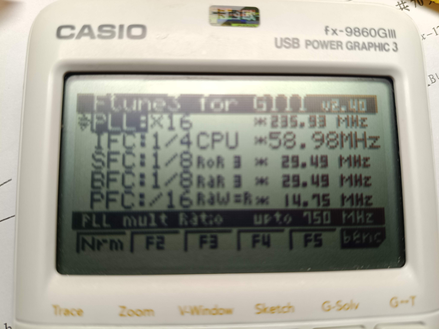
FLL:x900 * 14.75MHz
PLL:x16 *235.93MHz
IFC:1/4 CPU * 58.98MHz
SFC:1/8 RoR 3 * 29.49MHz
BFC:1/8 RaR 2 * 29.49MHz
PFC:/16 RaW =R * 14.75MHz
messeage area / benchmark score
[function key]
-----------------------------------
RoR: Number of ROM Wait Cycles in Read Access. color reverse: dangerous range.
RaR: Number of RAM Wait Cycles in Read Access. color reverse: dangerous range.
RaW: Number of RAM Wait Cycles in Write Access. color reverse: dangerous range.
-------------------------------------------------------------------------------
-[UP] select up (FLL,PLL,SFC,BFC,PFC)
-[DOWN] select down (FLL,PLL,SFC,BFC,PFC)
-[LEFT] decrement 1 step multiplication or divider
-[RIGHT] increment 1 step multiplication or divider
-[SHIFT]+[UP] select FLL multiplication ( =>setup select )
-[F1] Load normal default setting CPU 29MHz, PLLx16, bus 29MHz, default wait
-[F2] Recall [F2] setting preset CPU 59MHz, PLLx16, bus 29MHz, same as Prizm default
-[F3] Recall [F3] setting preset CPU 29MHz, PLLx16, bus 29MHz, same as SH3 model
-[F4] Recall [F4] setting preset CPU 118MHz, PLLx32, bus 59MHz, modified wait
-[F5] Recall [F5] setting preset CPU 236MHz, PLLx32, bus 118MHz, modified wait
-[F6] simple benchmark
CPUcore simple loop count per 100ms. ( 9860G add-in "UTIL" like )
and MEMORY(ROM,RAM,I/O) access loop count per 50ms
toggle more
CPUcore and PutDsipDD speed (fps)
-[SHIFT]
-[F1] Save setting to file (main memory). load data automatically on the next run.
-[F2] Store current setting to function KEY [F2]
-[F3] Store current setting to function KEY [F3]
-[F4] Store current setting to function KEY [F4]
-[F5] Store current setting to function KEY [F5]
-[F6] Load setting from file (main memory)
-[OPTN] List of bus frequency limit value table in each of wait.
-[F4] initialize default setting
-[F5] ROM & RAM / RAM WRITE & READ table chenge.
The limit frequency of the RAM does not increase from a certain spot,
but there becomes the limit of the SHW clock & bus clock.
-[F6] Auto check for memory speed in each of wait.
-[VARS]
-[F1] register display FRQCR,CCR
-[F2] register display BCR/WCR toggle
-[F3] modify CS0BCR CS2BCR
select cursor key
-[F1] +
-[F2] -
-[F4] initialize default setting
-[F4] modify CS0WCR CS2WCR
select cursor key
-[F1] +
-[F2] -
-[F4] initialize default setting
-[F5] modify CS5ABCR CS5BBCR
select cursor key
-[F1] +
-[F2] -
-[F4] initialize default setting
-[F6] modify CS5AWCR CS5BWCR
select cursor key
-[F1] +
-[F2] -
-[F4] initialize default setting
-[PRGM]
-[F1] modify CS3BCR CS4BCR
-[F2] modify CS3WCR CS4WCR
-[F3] modify CS5ABCR CS5BBCR
-[F4] modify CS5AWCR CS4BWCR
-[F5] modify CS6ABCR CS6BBCR
-[F6] modify CS6AWCR CS6BWCR
-[EXIT] exit
-[AC] default menu screen
-[EXE] if benchmark selected it is carried out once again.
- increment ROM wait
-[/] decrement ROM wait
When it may be lowered, memory check begins
if error,cannot decrement.
-[+] increment RAM wait
-[-] decrement RAM wait
When it may be lowered, memory check begins
if error,cannot decrement.
-[SHIFT]+[+] increment RAM WW wait "=R" same cycles as WR settings
-[SHIFT]+[-] decrement RAM WW wait "=R" same cycles as WR settings
-[SETUP] default setting
ROM Wait margin 0-15% 3% ( less than 1% is dangerous. ) not reset wait table.
RAM Wait margin 0-15% 3% ( less than 1% is dangerous. ) not reset wait table.
PLL frequency MAX 800MHz
CPU frequency MAX 285MHz
Shw frequency MAX 180MHz
Bus frequency MAX 134MHz
I/O frequency MAX 30MHz
Startup mem check on/off on
F1 yes/no check on/off off
Wait Auto decrement on/off on
RAM WW Auto inc/dec on/off on
ROM IWW Auto decrement on/off on
PFC Auto increment on/off on
FLL display noshift on/off off
BATT volt display on/off off
-------------------------------------------------------------------------------
Auto memory check
-------------------------------------------------------------------------------
It is an important point of this tool to measure speed of the memory.
At first,look for the slowest 64K block.
and check the upper limit in each wait.
Check it by performing a reading of the same address twice whether it is not different.
It is a read error if different.
the measurement of the write speed tests,
measure and acquire a speed difference revision level first.
read and write in a memory area of 4KB.
When with a USB power supply, 1%-3% become quick in the memory speed.
Please measure it in battery.
-------------------------------------------------------------------------------
Caution
-------------------------------------------------------------------------------
USB cannot recognize that bus clocks over about 130MHz.
I do not know the measures of this.
RS232C depends on the I/O clock.
When you communicate in two, please put I/O clocks together.
In the prizm,
when bus clocks over about 130MHz-150MHz, a screen collapses.
Please modify CS5ABCR or CS5AWCR.
increment IWW (CS5ABCR) or increment WW,SW,HW (CS5AWCR)
So it can be settled.
but turn off and turn on it do not return to a previous state. ( return default )
and bult-in overclocking games,
will freeze surely when operate it in PLL 26x or more.
-------------------------------------------------------------------------------
Acknowledgements
-------------------------------------------------------------------------------
This program was based on Pover(by Ashbad).
developed by PrizmSDK 0.3(Ptune2) & CASIO SDK(Ftune2).
fxReverse project documentation,
SuperH-based fx calculators,
Cemetech WikiPrizm,
served as a reference very much.
Very thanks for result of the analysis of all senior users.
I would be happy if this tool is useful for you.
-------------------------------------------------------------------------------
LICENCE
-------------------------------------------------------------------------------
This software is freeware.
The license follows GPLv2.
-------------------------------------------------------------------------------
v2.40 2020.2.20 Fixed the bug that the battery voltage display occured system error in the emulator.
Changed "X" display to multiplication symbol.
v2.30 2019.2.11 Newly supported fx-9860GIII/9750GIII.(only display)
v2.20 2019.8.31 Corrected the value of battery voltage display.
v2.02 2019.7.13 In the case of Graph 35+E II, fixed a bug that causes the screen receiver transfer error if the bus clock exceeds about 58 MHz.
v2.01 2019.7.12 In the case of Graph 35+E II, if the bus clock exceeds about 80 MHz, the LCD transfer will fail, so the default settings for [F4] and [F5] have been optimized.
And, the setting of CS5AWCR:SW is automatically changed by the rise of the bus clock.
v2.00 2019.7.7 Added support Graph 35+E II.
Supported models are judged automatically.
And it has been renamed to Ftune3.
v1.11a 2017.10.20 changed memory test value. ( When memory test error is given in previous version, please try this version.)
v1.11 2016. 7.31 corrected version display errors. (1.10->1.11)
2016. 7.21 Changed memory test including a hidden RAM area.(upper 256KB)
v1.10 2016. 4.24 It is not required re-measurement when changed memory wait margin setting by setup.
Change default memory speed frequency table.
v1.02 2015. 6.20 Check the CPU type at first.
It does not start when it is SH3.
changed some icon designs to be easy to distinguish it from Ftune(SH3)
v1.01 2015. 2.28 To solve problems in memtest failure.(When PLL limit is low, and memory limit is high.)
renewed some source codes. as a result, file size decreased.
v1.00b 2014.12.21 fixed benchmark result of CPU.(adjustment alignment)
RAM write safety zone (reverse dsp) 90%->95%.
default preset change F3:same as SH3.
v1.00a 2014.11.27 There is not any change operatively.
only fixed careless miss...
v1.00 2014.11.14 first release
机翻:
===============================================================================
Ftune3 是用于 fx-9860GIII / Graph 35+E II 的 SH7305 CPG&BSC 调谐工具 版本 2.40
版权所有 (c) 2014/2015-2020,作者:sentaro21
电子邮箱:[email protected]
===============================================================================
PRIZM 和 fx-9860GIII 使用的 CPU 是称为 SH7305 的 SH4A CPU。
它与 SH7724 相似。
此工具用于修改 CPG(时钟脉冲发生器)和 BSC(总线状态控制器)。
功能:
让你的计算器进入超过 200MHz 的世界!!
自动进行内存速度测试。
使用功能键存储和调用频率/等待设置。
将设置保存到文件(主内存)。下次运行时自动加载数据。
缺点:
此工具的测试尚不充分。
可能会发生意外的故障。
超频时电池消耗会显著增加。
====== 警告!!! =============================================================
此工具旨在安全运行,但可能会发生未知故障。
此工具可能对你的计算器造成损坏!
请自行承担使用风险。
对任何损坏概不负责。
CPG(时钟脉冲发生器) 引用:SH7724 数据手册
FLL:FLL 电路倍频比。
FLL 电路对从 RTC_CLK 输入的时钟频率(32.768KHz)进行倍频。
默认倍频比为 900。
FLL 电路输出:32768Hz*900/2=14.7456MHz
这与旧款 SH3 模型的振荡频率相同。
PLL:PLL 电路倍频比。
基准频率为 FLL 输出的 14.7456MHz
倍频比为 1-64
当频率超过约 800MHz 时,速度会减半。
(PLL 时钟最高约 750MHz)
IFC:CPU 时钟分频比。
默认分频比为 1/8,频率为 29.49MHz。
SFC:SHW 时钟分频比。
默认分频比为 1/8,频率为 29.49MHz。
BFC:总线时钟分频比。
默认分频比为 1/8,频率为 29.49MHz。
当总线时钟超过约 130MHz 时,USB 可能无法识别。
PFC:I/O 时钟分频比。
默认分频比为 1/16,频率为 14.75MHz。
即使超过 40MHz 也可能工作,但会影响闪存性能。
设置为尽可能接近默认值的频率是安全的。(建议低于 30MHz)
分频比(与 SH7724 不完全相同)
0000: 1/2
0001: 1/4
0010: 1/8 IFC, SFC, BFC 默认值
0011: 1/16 PFC 默认值
0100: 1/32
0101: 1/64
注意:
IFC >= SFC >= BFC >= PFC
IFC:SFC 仅支持 1:1 或 1:2
此工具会自动调整。
BSC(总线状态控制器) 引用:SH7724 数据手册
BCR/WCR 的寄存器结构与 SH7724 相似。
CS0BCR, CS0WCR :FLASH ROM 区域
CS2BCR, CS2WCR :主 RAM 区域
CS5ABCR,CS5AWCR :LCDC
其他未知。
CSn 空间总线控制寄存器 (CSnBCR) (n=0,2,3,4,5A,5B,6A,6B)
IWW:指定写-读/写-写周期之间的空闲周期数。
000: 无空闲周期
001: 插入 1 个空闲周期
010: 插入 2 个空闲周期
011: 插入 4 个空闲周期
100: 插入 6 个空闲周期
101: 插入 8 个空闲周期
110: 插入 10 个空闲周期
111: 插入 12 个空闲周期
(CS0BCR,CS2BCR)@SH7305 默认值为插入 2 个空闲周期。
频率较低时可设置为更低的数值。
效果显著。
IWRWD:指定不同空间之间的读-写周期空闲周期数。
000: 无空闲周期
001: 插入 1 个空闲周期
010: 插入 2 个空闲周期
011: 插入 4 个空闲周期
100: 插入 6 个空闲周期
101: 插入 8 个空闲周期
110: 插入 10 个空闲周期
111: 插入 12 个空闲周期
(CS0BCR,CS2BCR)@SH7305 默认值为插入 2 个空闲周期。
频率较低时可设置为更低的数值。
有效,但效果不明显。
IWRWS:指定同一空间内的读-写周期空闲周期数。
000: 无空闲周期
001: 插入 1 个空闲周期
010: 插入 2 个空闲周期
011: 插入 4 个空闲周期
100: 插入 6 个空闲周期
101: 插入 8 个空闲周期
110: 插入 10 个空闲周期
111: 插入 12 个空闲周期
(CS0BCR,CS2BCR)@SH7305 默认值为插入 2 个空闲周期。
频率较低时可设置为更低的数值。
有效,但效果不明显。
IWRRD:指定不同空间之间的读-读周期空闲周期数。
000: 无空闲周期
001: 插入 1 个空闲周期
010: 插入 2 个空闲周期
011: 插入 4 个空闲周期
100: 插入 6 个空闲周期
101: 插入 8 个空闲周期
110: 插入 10 个空闲周期
111: 插入 12 个空闲周期
(CS0BCR,CS2BCR)@SH7305 默认值为插入 2 个空闲周期。
频率较低时可设置为更低的数值。
有效,但效果不明显。
IWRRS:指定同一空间内的读-读周期空闲周期数。
000: 无空闲周期
001: 插入 1 个空闲周期
010: 插入 2 个空闲周期
011: 插入 4 个空闲周期
100: 插入 6 个空闲周期
101: 插入 8 个空闲周期
110: 插入 10 个空闲周期
111: 插入 12 个空闲周期
(CS0BCR,CS2BCR)@SH7305 默认值为插入 2 个空闲周期。
频率较低时可设置为更低的数值。
效果显著。
CSn 空间等待控制寄存器 (CSnWCR) (n=0,2,3,4,5A,5B,6A,6B)
WW:写访问等待周期数
000: 与 WR 设置相同
001: 0 周期
010: 1 周期
011: 2 周期
100: 3 周期
101: 4 周期
110: 5 周期
111: 6 周期
(CS0WCR,CS2WCR)@SH7305 默认值与 WR 设置相同。
我认为无需更改。
但独立设置可以加快内存访问速度。
CS5AWCR 效果显著。(当 LCD 出现异常时)
WR:读访问等待周期数
0000: 0 周期 1000: 10 周期
0001: 1 周期 1001: 12 周期
0010: 2 周期 1010: 14 周期
0011: 3 周期 1011: 18 周期
0100: 4 周期 1100: 24 周期
0101: 5 周期
0110: 6 周期
0111: 8 周期
CS0WCR@PRIZM 默认值为 3 周期
CS0WCR@9860GII-2 默认值为 18 周期
增加此值可提升总线频率。
CS2WCR@SH7305 默认值为 2 周期
增加此值可提升总线频率。
SW:从地址、CSn 确认到 RD、WE 确认的延迟周期数。
00: 0.5 周期
01: 1.5 周期
10: 2.5 周期
11: 3.5 周期
(CS0WCR,CS2WCR)@SH7305 默认值为 0.5 周期。
HW:从 RD、WEn 取消确认到地址、CSn 取消确认的延迟周期数。
00: 0.5 周期
01: 1.5 周期
10: 2.5 周期
11: 3.5 周期
(CS0WCR,CS2WCR)@SH7305 默认值为 0.5 周期。
默认设置下,内存总线频率限制了 CPU 核心频率。
fx-9860GII-2 型号 ROM 18等待 RAM 2等待 (默认)
默认情况下 ROM 频率最高可达 180MHz(18 等待)
RAM 频率最高约 70MHz-75MHz(取决于未知的 SRAM 芯片)
此工具可以修改等待状态,
如果增加等待状态,可以提升内存总线频率。
从而提升计算器性能。
CPU 时钟最高 265-300MHz(安全范围约 260MHz)
SHW 时钟最高 175-200MHz(安全范围约 160MHz)
总线时钟最高 175-200MHz(安全范围约 120MHz)
I/O 时钟最高 - 40MHz(安全范围约 30MHz)
(限制因个体差异而不同。)
核心时钟对小程序有效。
整体性能受总线时钟影响。
====== 警告!!! =============================================================
此工具旨在安全运行,但可能会发生未知故障。
此工具可能对你的计算器造成损坏!
请自行承担使用风险。
对任何损坏概不负责。
使用方法
主屏幕
FLL:x900 * 14.75MHz
PLL:x16 *235.93MHz
IFC:1/4 CPU * 58.98MHz
SFC:1/8 RoR 3 * 29.49MHz
BFC:1/8 RaR 2 * 29.49MHz
PFC:/16 RaW =R * 14.75MHz
消息区域 / 基准测试分数
[功能键]
RoR: ROM 读访问等待周期数。 颜色反显:危险范围。
RaR: RAM 读访问等待周期数。 颜色反显:危险范围。
RaW: RAM 写访问等待周期数。 颜色反显:危险范围。
-[上] 向上选择(FLL, PLL, SFC, BFC, PFC)
-[下] 向下选择(FLL, PLL, SFC, BFC, PFC)
-[左] 倍频或分频值减少 1 步
-[右] 倍频或分频值增加 1 步
-[SHIFT]+[上] 选择 FLL 倍频(=> 进入设置选择)
-[F1] 加载正常默认设置 CPU 29MHz, PLLx16, 总线 29MHz, 默认等待
-[F2] 调用 [F2] 设置 预设 CPU 59MHz, PLLx16, 总线 29MHz, 同 Prizm 默认
-[F3] 调用 [F3] 设置 预设 CPU 29MHz, PLLx16, 总线 29MHz, 同 SH3 模型
-[F4] 调用 [F4] 设置 预设 CPU 118MHz, PLLx32, 总线 59MHz, 修改后的等待
-[F5] 调用 [F5] 设置 预设 CPU 236MHz, PLLx32, 总线 118MHz, 修改后的等待
-[F6] 简单基准测试
CPU 核心在 100ms 内的简单循环计数。(类似 9860G 插件 "UTIL")
以及内存(ROM, RAM, I/O)访问在 50ms 内的循环计数
多次切换
CPU 核心和 PutDsipDD 速度
-[SHIFT]
-[F1] 将设置保存到文件(主内存)。下次运行时自动加载。
-[F2] 将当前设置存储到功能键 [F2]
-[F3] 将当前设置存储到功能键 [F3]
-[F4] 将当前设置存储到功能键 [F4]
-[F5] 将当前设置存储到功能键 [F5]
-[F6] 从文件(主内存)加载设置
-[OPTN] 各等待状态下总线频率限制值列表
-[F4] 初始化为默认设置
-[F5] ROM & RAM / RAM 写和读 表切换。
RAM 的限制频率不会从某点再增加,
但会受到 SHW 时钟和总线时钟的限制。
-[F6] 自动检查各等待状态下的内存速度。
-[VARS]
-[F1] 寄存器显示 FRQCR, CCR
-[F2] 寄存器显示 BCR/WCR 切换
-[F3] 修改 CS0BCR CS2BCR
使用方向键选择
-[F1] +
-[F2] -
-[F4] 初始化为默认设置
-[F4] 修改 CS0WCR CS2WCR
使用方向键选择
-[F1] +
-[F2] -
-[F4] 初始化为默认设置
-[F5] 修改 CS5ABCR CS5BBCR
使用方向键选择
-[F1] +
-[F2] -
-[F4] 初始化为默认设置
-[F6] 修改 CS5AWCR CS5BWCR
使用方向键选择
-[F1] +
-[F2] -
-[F4] 初始化为默认设置
-[PRGM]
-[F1] 修改 CS3BCR CS4BCR
-[F2] 修改 CS3WCR CS4WCR
-[F3] 修改 CS5ABCR CS5BBCR
-[F4] 修改 CS5AWCR CS4BWCR
-[F5] 修改 CS6ABCR CS6BBCR
-[F6] 修改 CS6AWCR CS6BWCR
-[EXIT] 退出
-[AC] 返回默认菜单屏幕
-[EXE] 如果已选择基准测试,则再次运行。
- 增加 ROM 等待
-[/] 减少 ROM 等待
当可能降低时,开始内存检查
如果出错,则无法减少。
-[+] 增加 RAM 等待
-[-] 减少 RAM 等待
当可能降低时,开始内存检查
如果出错,则无法减少。
-[SHIFT]+[+] 增加 RAM WW 等待 "=R" 与 WR 设置相同周期数
-[SHIFT]+[-] 减少 RAM WW 等待 "=R" 与 WR 设置相同周期数
-[SETUP] 默认设置
ROM 等待裕度 0-15% 3% (低于 1% 危险。)不重置等待表。
RAM 等待裕度 0-15% 3% (低于 1% 危险。)不重置等待表。
PLL 频率最大值 800MHz
CPU 频率最大值 285MHz
Shw 频率最大值 180MHz
总线频率最大值 134MHz
I/O 频率最大值 30MHz
启动时内存检查 开/关 开
F1 是/否检查 开/关 关
等待自动减少 开/关 开
RAM WW 自动增/减 开/关 开
ROM IWW 自动减少 开/关 开
PFC 自动增加 开/关 开
FLL 显示不移位 开/关 关
电池电压显示 开/关 关
自动内存检查
此工具的一个重要点是测量内存速度。
首先,寻找最慢的 64K 块。
并检查各等待状态下的上限。
通过执行两次相同地址的读取操作来检查是否一致。
如果不一致,则为读取错误。
写入速度的测量测试,
首先测量并获取速度差异修正值。
在 4KB 的内存区域进行读写。
当使用 USB 供电时,内存速度会加快 1%-3%。
请使用电池进行测量。
注意事项
当总线时钟超过约 130MHz 时,USB 可能无法识别。
我不知道此问题的解决方法。
RS232C 依赖于 I/O 时钟。
当进行双向通信时,请将 I/O 时钟设置为一致。
在 prizm 上,
当总线时钟超过约 130MHz-150MHz 时,屏幕会异常。
请修改 CS5ABCR 或 CS5AWCR。
增加 IWW 或增加 WW, SW, HW
这样可以解决问题。
但关机再开机不会恢复到之前的状态。(会返回默认值)
并且内置的超频游戏,
在 PLL 26x 或更高频率下运行时会必定冻结。
致谢
此程序基于 Pover(作者:Ashbad)。
使用 PrizmSDK 0.3 和 CASIO SDK 开发。
fxReverse 项目文档、
基于 SuperH 的 fx 计算器、
Cemetech WikiPrizm、
提供了大量参考。
非常感谢所有资深用户的分析成果。
希望此工具对您有用。
许可证
此软件是免费软件。
遵循 GPLv2 许可证。
v2.40 2020.2.20 修复了在模拟器中电池电压显示导致系统错误的 bug。
将 "X" 显示改为乘号。
v2.30 2019.2.11 新增支持 fx-9860GIII/9750GIII。(仅显示)
v2.20 2019.8.31 修正了电池电压显示的值。
v2.02 2019.7.13 修复了在 Graph 35+E II 上,如果总线时钟超过约 58 MHz 会导致屏幕接收器传输错误的 bug。
v2.01 2019.7.12 在 Graph 35+E II 上,如果总线时钟超过约 80 MHz,LCD 传输会失败,因此优化了 [F4] 和 [F5] 的默认设置。
并且,CS5AWCR:SW 的设置会根据总线时钟的升高自动更改。
v2.00 2019.7.7 增加对 Graph 35+E II 的支持。
支持的型号会自动判断。
并更名为 Ftune3。
v1.11a 2017.10.20 更改了内存测试值。(如果旧版本出现内存测试错误,请尝试此版本。)
v1.11 2016. 7.31 修正了版本显示错误。(1.10->1.11)
2016. 7.21 更改了内存测试,包括隐藏的 RAM 区域。(高 256KB)
v1.10 2016. 4.24 当通过设置更改内存等待裕度时,无需重新测量。
更改默认内存速度频率表。
v1.02 2015. 6.20 启动时检查 CPU 类型。
如果是 SH3 则不启动。
更改了一些图标设计,以便与 Ftune 区分。
v1.01 2015. 2.28 解决了内存测试失败的问题。(当 PLL 限制低而内存限制高时。)
更新了部分源代码。结果文件大小减小了。
v1.00b 2014.12.21 修正了 CPU 基准测试结果。(调整对齐)
RAM 写入安全区(反色显示)90%->95%。
更改默认预设 F3:与 SH3 相同。
v1.00a 2014.11.27 操作上无任何变化。
仅修正了粗心错误...
v1.00 2014.11.14 首次发布。
|
|




 发表于 2025-11-10 12:16:01

 沉默卡
沉默卡 变色卡
变色卡 千斤顶
千斤顶 显身卡
显身卡
 楼主
楼主